
Mode Register
The mode register is used to define the specific mode of operation of the DDR2 SDRAM.
Mode register는 DDR2 SDRAM의 특정 모드를 정의하는데 사용한다.
This definition includes the selection of a burst length, burst type, CAS latency, operating mode, DLL RESET, write recovery, and power-down mode, as shown in Figure 36.
burst length, burst type, CAS latency, operating mode, DLL RESET, write recovery, and power-down mode을 선택한다. Figure36 참조

Contents of the mode register can be altered by re-executing the LOAD MODE (LM) command.
Mode Register의 내용은 LOAD MODE (LM) 명령을 다시 실행하여 변경 가능
If the user chooses to modify only a subset of the MR variables, all variables must be programmed when the command is issued.
사용자가 MR변수의 일부만 수정하기로 선택하면, 명령이 발행할 때 모든 변수가 프로그램되어야 한다.
The MR is programmed via the LM command and will retain the stored information until it is programmed again or until the device loses power (except for bit M8, which is self-clearing).
MR(Mode register)은 LM Command를 통해 프로그래밍되고 다시 프로그래밍되거나 장치가 전원이 꺼질 때까지 저장된 정보를 유지할 것이다,(self-clearing인 M8은 제외)
Reprogramming the mode register will not alter the contents of the memory array, provided it is performed correctly.
Mode register를 올바르게 재프로그래밍하면 메모리 배열의 내용을 변경되지 않습니다.
The LM command can only be issued (or reissued) when all banks are in the precharged state (idle state) and no bursts are in progress.
LM Command은 오직 모든 bank가 precharge(또는 idle)이거나 어떤한 burst도 진행 중이지 않을 때 실행되거나 재실행할수 있다.
The controller must wait the specified time tMRD before initiating any subsequent operations such as an ACTIVATE command.
controller는 ACTIVATE Command와 같은 작업이 시작하기 전에 tMRD를 기다려야 한다.
Violating either of these requirements will result in an unspecified operation.
이러한 요구 사항 중 어느 하나라도 위반하면 정의되지 않은 작업이 발생할 것이다.
Burst Length
Burst length is defined by bits M0-M2, as shown in Figure 36.
Burst Length는 bit M0-M2에 의해 정의됩니다. Figure 36 참조

Read and write accesses to the DDR2 SDRAM are burst-oriented, with the burst length being programmable to either four or eight.
DDR2 SDRAM에 대한 READ, WRITE는 burst 방식을 지향한다. burst length는 4, 8개로 프로그래밍 가능하다.
The burst length determines the maximum number of column locations that can be accessed for a given READ or WRITE command.
burst length는 지정된 READ, WRITE Command를 할 수 있는 최대 열 위치 수를 결정한다.
When a READ or WRITE command is issued, a block of columns equal to the burst length is effectively selected.
READ, WRITE Command가 실행되면, burst length와 동일한 열 블록이 선택된다.
All accesses for that burst take place within this block, meaning that the burst will wrap within the block if a boundary is reached.
burst에 대한 모든 접근은 burst length와 동일한 열 블록 내에서 발생하며, 이는 경계에 도달하면 burst는 block 내에서 wrap된다.(wrap : 동일한 블록의 시작 부분으로 순환)
The block is uniquely selected by A2-Ai when BL = 4 and by A3-Ai when BL = 8 (where Ai is the most significant column address bit for a given configuration).
BL = 4일 때 블록은 A2-Ai에 의해 고유하게 선택됩니다, 그리고 그리고 BL = 8일 때는 A3-Ai에 의해 선택됩니다.(여기서 Ai는 주어진 구성에 대한 최상위 열 주소 비트입니다).
The remaining (least significant) address bit(s) is (are) used to select the starting location within the block.
나머지(최하위) 주소 비트는 블록 내 시작 위치를 선택하는 데 사용됩니다.
The programmed burst length applies to both read and write bursts.
프로그래밍된 burst length는 read, write burst에 모두 적용된다.
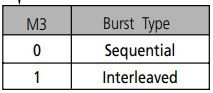
Burst Type
Accesses within a given burst may be programmed to be either sequential or interleaved.
burst는 sequential 이나 interleaved로 프로그래밍 가능하다.
The burst type is selected via bit M3, as shown in Figure 36.
버스트 유형은 그림 36과 같이 비트 M3을 통해 선택됩니다.
The ordering of accesses within a burst is determined by the burst length, the burst type, and the starting column address, as shown in Table 41.
버스트 내 액세스 순서는 burst length, burst type 및 시작 열 주소에 의해 결정됩니다. 열 주소에 의해 결정됩니다(표 41 참조).
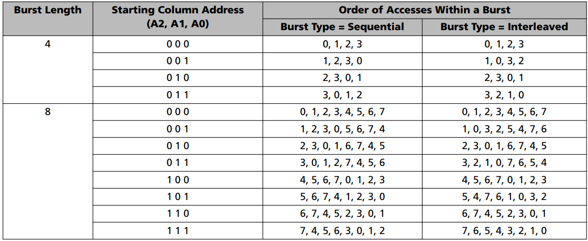
DDR2 SDRAM supports 4-bit burst mode and 8-bit burst mode only.
DDR2 SDRAM은 4비트 버스트 모드와 8비트 버스트 모드만 지원합니다.
For 8-bit burst mode, full interleaved address ordering is supported; however, sequential address ordering is nibble-based.
8-bit burst mode경우 전부 interleaved 주소 정렬을 지원하지만, sequential 주소 정렬은 nibble(4bit) 기반이다.
Operating Mode
The normal operating mode is selected by issuing a command with bit M7 set to "0," and all other bits set to the desired values, as shown in Figure 36.
normal operating mode는 M7 bit를 0으로 설정하여 선택한다. 그리고 다른 모든 bit를 원하는 값으로 설정한다(Figure 36 참조).

When bit M7 is “1,” no other bits of the mode register are programmed.
bit M7이 "1"이면 모드 레지스터의 다른 비트는 프로그래밍되지 않습니다.
Programming bit M7 to “1” places the DDR2 SDRAM into a test mode that is only used by the manufacturer and should not be used.
비트 M7을 "1"로 프로그래밍하면 DDR2 SDRAM이 제조업체에서만 사용하며 사용해서는 안 되는 test mode로 전환됩니다.
No operation or functionality is guaranteed if M7 bit is "1".
M7 비트가 "1"인 경우 작동 또는 기능이 보장되지 않습니다.
DLL RESET
DLL RESET is defined by bit M8, as shown in Figure 36.
DLL RESET은 비트 M8로 정의됩니다.

Programming bit M8 to “1” will activate the DLL RESET function.
비트 M8을 "1"로 프로그래밍하면 DLL RESET 기능이 활성화됩니다.
Bit M8 is self-clearing, meaning it returns back to a value of "0" after the DLL RESET function has been issued.
비트 M8은 self-clearing이므로 DLL RESET 함수가 실행된 후 다시 "0" 값으로 돌아갑니다.
Anytime the DLL RESET function is used, 200 clock cycles must occur before a READ command can be issued to allow time for the internal clock to be synchronized with the external clock.
DLL RESET 기능이 사용될 때마다 내부 clock이 외부 clock과 동기화될 수 있도록 시간을 확보하기 위해 READ Command가 실행되지 전에 200 clock cycle이 발생해야 한다.
Failing to wait for synchronization to occur may result in a violation of the tAC or tDQSCK parameters.
동기화가 이루어질 때까지 기다리지 않으면 tAC 또는 tDQSCK 매개 변수가 위반될 수 있습니다.
Delay-Locked Loop (DLL)을 재설정하는 데 사용됩니다. DLL은 메모리 칩 내부의 클럭 신호를 외부의 클럭 신호와 동기화하는 데 사용되는 회로입니다.
Write Recovery
Write recovery (WR) time is defined by bits M9–M11, as shown in Figure 36.
WR(Write recovery) 시간은 Figure 36과 같이 비트 M9-M11에 의해 정의됩니다.

The WR register is used by the DDR2 SDRAM during WRITE with auto precharge operation.
WR register는 auto precharge 작동을 통한 WRITE 중에 DDR2 SDRAM에서 사용됩니다.
During WRITE with auto precharge operation, the DDR2 SDRAM delays the internal auto precharge operation by WR clocks (programmed in bits M9–M11) from the last data burst.
auto precharge가 있는 WRITE 동안 DDR2 SDRAM은 마지막 데이터 burst에서 WR clock(bit M9-M11로 프로그래밍됨)에 의해 내부 auto precharge을 지연시킨다.
An example of WRITE with auto precharge is shown in Figure 65.
Figure 65에는 auto precharge 기능이 있는 WRITE의 예가 나와 있습니다.

WR values of 2, 3, 4, 5, 6, 7, or 8 clocks may be used for programming bits M9–M11.
2, 3, 4, 5, 6, 7, 8 클럭의 WR 값은 비트 M9-M11을 프로그래밍하는 데 사용할 수 있다.
The user is required to program the value of WR, which is calculated by dividing tWR (in nanoseconds) by tCK (in nanoseconds) and rounding up a noninteger value to the next integer; WR (cycles) = tWR (ns)/tCK (ns).
사용자는 tWR(나노초)을 tCK(나노초)로 나누고 정수가 아닌 값을 다음 정수로 반올림하여 계산되는 WR 값을 프로그래밍해야 합니다(WR(주기) = tWR(ns)/tCK(ns)).
Reserved states should not be used as an unknown operation or incompatibility with future versions may result.
Reserved 상태는 알 수 없는 연산으로 사용해서는 안 되며, 향후 버전과 호환되지 않을 수 있습니다.
Power-Down Mode
Active power-down (PD) mode is defined by bit M12, as shown in Figure 36.
Active power-down mode(PD)는 비트 M12로 정의한다. (Figure 36 참조)

PD mode enables the user to determine the active power-down mode, which determines performance versus power savings.
PD 모드를 통해 사용자는 성능과 전력 절감을 결정하는 active power-down mode를 결정할 수 있습니다.
PD mode bit M12 does not apply to precharge PD mode.
PD 모드 비트 M12는 precharge PD 모드에는 적용되지 않습니다.
When bit M12 = 0, standard active PD mode, or “fast-exit” active PD mode, is enabled.
비트 M12 = 0이면 standard active PD mode 또는 "fast-exit" 활성 PD 모드가 활성화됩니다.
The tXARD parameter is used for fast-exit active PD exit timing.
tXARD parameter는 fast-exit active PD exit 타이밍에 사용됩니다.
The DLL is expected to be enabled and running during this mode.
이 모드에서는 DLL이 활성화되어 실행할 것을 요구한다.
When bit M12 = 1, a lower-power active PD mode, or "slow-exit" active PD mode, is enabled.
비트 M12 = 1이면 lower-power active PD mode 또는 "slow-exit" active PD mode가 활성화됩니다.
The tXARDS parameter is used for slow-exit active PD exit timing.
tXARDS 파라미터는 slow-exit active PD exit에 사용됩니다.
The DLL can be enabled but "frozen" during active PD mode because the exit-to-READ command timing is relaxed.
DLL은 활성화할 수 있지만 active PD mode에서는 종료에서 exit-to-READ Command 타이밍이 유연함으로 "frozen"될 수 있습니다.
"frozen"이라는 표현은 DLL이 활성화되어 있지만, 그 기능이 일시적으로 중지되어 있다는 것을 의미
메모리 칩이 일반 작동 상태로 복귀한 직후에 즉시 READ 명령을 수행할 필요가 없고, 일정 시간 간격을 두고 READ 명령을 수행할 수 있다는 것
The power difference expected between IDD3P normal and IDD3P lowpower mode is defined in the DDR2 IDD Specifications and Conditions table.
IDD3P 일반 모드와 IDD3P 저전력 모드 간에 예상되는 전력 차이는 DDR2 IDD 사양 및 조건 표에 정의되어 있습니다.
CAS Latency(CL)
The CAS latency (CL) is defined by bits M4–M6, as shown in Figure 36.
CAS 대기 시간(CL)은 그림 36에 표시된 것처럼 비트 M4-M6으로 정의됩니다.

CL is the delay, in clock cycles, between the registration of a READ command and the availability of the first bit of output data.
CL은 READ 명령을 등록한 후 첫 번째 출력 데이터 비트가 사용 가능해지기까지의 clock cycle의 지연시간입니다.
The CL can be set to 3, 4, 5, 6, or 7 clocks, depending on the speed grade option being used.
사용 중인 속도 등급 옵션에 따라, CL은 3, 4, 5, 6, 또는 7 클럭으로 설정될 수 있습니다.
DDR2 SDRAM does not support any half-clock latencies.
DDR2 SDRAM은 half-clock latency를 지원하지 않습니다.
Reserved states should not be used as an unknown operation otherwise incompatibility with future versions may result.
Reserved states는 알 수 없는 작업으로 사용되어서는 안 되며, 그렇게 사용될 경우 미래 버전과의 호환성 문제가 발생할 수 있습니다.
DDR2 SDRAM also supports a feature called posted CAS additive latency (AL).
DDR2 SDRAM은 'posted CAS additive latency (AL)'이라는 기능도 지원합니다.
This feature allows the READ command to be issued prior to tRCD (MIN) by delaying the internal command to the DDR2 SDRAM by AL clocks.
이 기능은 AL 클럭만큼 내부 명령을 지연시킴으로써, READ 명령을 tRCD (MIN) 이전에 발행할 수 있게 합니다."
The AL feature is described in further detail in Posted CAS Additive Latency (AL)
AL 기능에 대한 자세한 내용은 Posted CAS Additive Latency(AL)에 설명되어 있습니다.
Examples of CL = 3 and CL = 4 are shown in Figure 37; both assume AL = 0.
CL = 3 및 CL = 4의 예는 Figure 37에 나와 있으며, 둘 다 AL = 0으로 가정합니다.
If a READ command is registered at clock edge n, and the CL is m clocks, the data will be available nominally coincident with clock edge n + m (this assumes AL = 0).
만약 READ 명령이 n번째 클럭 엣지에서 등록되고, CL이 m 클럭이라면, 데이터는 원칙적으로 n + m번째 클럭 엣지와 동시에 사용 가능하게 됩니다 (이는 AL이 0이라고 가정할 때의 상황입니다).

Mode Register
The mode register is used to define the specific mode of operation of the DDR2 SDRAM.
Mode register는 DDR2 SDRAM의 특정 모드를 정의하는데 사용한다.
This definition includes the selection of a burst length, burst type, CAS latency, operating mode, DLL RESET, write recovery, and power-down mode, as shown in Figure 36.
burst length, burst type, CAS latency, operating mode, DLL RESET, write recovery, and power-down mode을 선택한다. Figure36 참조
Contents of the mode register can be altered by re-executing the LOAD MODE (LM) command.
Mode Register의 내용은 LOAD MODE (LM) 명령을 다시 실행하여 변경 가능
If the user chooses to modify only a subset of the MR variables, all variables must be programmed when the command is issued.
사용자가 MR변수의 일부만 수정하기로 선택하면, 명령이 발행할 때 모든 변수가 프로그램되어야 한다.
The MR is programmed via the LM command and will retain the stored information until it is programmed again or until the device loses power (except for bit M8, which is self-clearing).
MR(Mode register)은 LM Command를 통해 프로그래밍되고 다시 프로그래밍되거나 장치가 전원이 꺼질 때까지 저장된 정보를 유지할 것이다,(self-clearing인 M8은 제외)
Reprogramming the mode register will not alter the contents of the memory array, provided it is performed correctly.
Mode register를 올바르게 재프로그래밍하면 메모리 배열의 내용을 변경되지 않습니다.
The LM command can only be issued (or reissued) when all banks are in the precharged state (idle state) and no bursts are in progress.
LM Command은 오직 모든 bank가 precharge(또는 idle)이거나 어떤한 burst도 진행 중이지 않을 때 실행되거나 재실행할수 있다.
The controller must wait the specified time tMRD before initiating any subsequent operations such as an ACTIVATE command.
controller는 ACTIVATE Command와 같은 작업이 시작하기 전에 tMRD를 기다려야 한다.
Violating either of these requirements will result in an unspecified operation.
이러한 요구 사항 중 어느 하나라도 위반하면 정의되지 않은 작업이 발생할 것이다.
Burst Length
Burst length is defined by bits M0-M2, as shown in Figure 36.
Burst Length는 bit M0-M2에 의해 정의됩니다. Figure 36 참조
Read and write accesses to the DDR2 SDRAM are burst-oriented, with the burst length being programmable to either four or eight.
DDR2 SDRAM에 대한 READ, WRITE는 burst 방식을 지향한다. burst length는 4, 8개로 프로그래밍 가능하다.
The burst length determines the maximum number of column locations that can be accessed for a given READ or WRITE command.
burst length는 지정된 READ, WRITE Command를 할 수 있는 최대 열 위치 수를 결정한다.
When a READ or WRITE command is issued, a block of columns equal to the burst length is effectively selected.
READ, WRITE Command가 실행되면, burst length와 동일한 열 블록이 선택된다.
All accesses for that burst take place within this block, meaning that the burst will wrap within the block if a boundary is reached.
burst에 대한 모든 접근은 burst length와 동일한 열 블록 내에서 발생하며, 이는 경계에 도달하면 burst는 block 내에서 wrap된다.(wrap : 동일한 블록의 시작 부분으로 순환)
The block is uniquely selected by A2-Ai when BL = 4 and by A3-Ai when BL = 8 (where Ai is the most significant column address bit for a given configuration).
BL = 4일 때 블록은 A2-Ai에 의해 고유하게 선택됩니다, 그리고 그리고 BL = 8일 때는 A3-Ai에 의해 선택됩니다.(여기서 Ai는 주어진 구성에 대한 최상위 열 주소 비트입니다).
The remaining (least significant) address bit(s) is (are) used to select the starting location within the block.
나머지(최하위) 주소 비트는 블록 내 시작 위치를 선택하는 데 사용됩니다.
The programmed burst length applies to both read and write bursts.
프로그래밍된 burst length는 read, write burst에 모두 적용된다.
Burst Type
Accesses within a given burst may be programmed to be either sequential or interleaved.
burst는 sequential 이나 interleaved로 프로그래밍 가능하다.
The burst type is selected via bit M3, as shown in Figure 36.
버스트 유형은 그림 36과 같이 비트 M3을 통해 선택됩니다.
The ordering of accesses within a burst is determined by the burst length, the burst type, and the starting column address, as shown in Table 41.
버스트 내 액세스 순서는 burst length, burst type 및 시작 열 주소에 의해 결정됩니다. 열 주소에 의해 결정됩니다(표 41 참조).
DDR2 SDRAM supports 4-bit burst mode and 8-bit burst mode only.
DDR2 SDRAM은 4비트 버스트 모드와 8비트 버스트 모드만 지원합니다.
For 8-bit burst mode, full interleaved address ordering is supported; however, sequential address ordering is nibble-based.
8-bit burst mode경우 전부 interleaved 주소 정렬을 지원하지만, sequential 주소 정렬은 nibble(4bit) 기반이다.
Operating Mode
The normal operating mode is selected by issuing a command with bit M7 set to "0," and all other bits set to the desired values, as shown in Figure 36.
normal operating mode는 M7 bit를 0으로 설정하여 선택한다. 그리고 다른 모든 bit를 원하는 값으로 설정한다(Figure 36 참조).
When bit M7 is “1,” no other bits of the mode register are programmed.
bit M7이 "1"이면 모드 레지스터의 다른 비트는 프로그래밍되지 않습니다.
Programming bit M7 to “1” places the DDR2 SDRAM into a test mode that is only used by the manufacturer and should not be used.
비트 M7을 "1"로 프로그래밍하면 DDR2 SDRAM이 제조업체에서만 사용하며 사용해서는 안 되는 test mode로 전환됩니다.
No operation or functionality is guaranteed if M7 bit is "1".
M7 비트가 "1"인 경우 작동 또는 기능이 보장되지 않습니다.
DLL RESET
DLL RESET is defined by bit M8, as shown in Figure 36.
DLL RESET은 비트 M8로 정의됩니다.
Programming bit M8 to “1” will activate the DLL RESET function.
비트 M8을 "1"로 프로그래밍하면 DLL RESET 기능이 활성화됩니다.
Bit M8 is self-clearing, meaning it returns back to a value of "0" after the DLL RESET function has been issued.
비트 M8은 self-clearing이므로 DLL RESET 함수가 실행된 후 다시 "0" 값으로 돌아갑니다.
Anytime the DLL RESET function is used, 200 clock cycles must occur before a READ command can be issued to allow time for the internal clock to be synchronized with the external clock.
DLL RESET 기능이 사용될 때마다 내부 clock이 외부 clock과 동기화될 수 있도록 시간을 확보하기 위해 READ Command가 실행되지 전에 200 clock cycle이 발생해야 한다.
Failing to wait for synchronization to occur may result in a violation of the tAC or tDQSCK parameters.
동기화가 이루어질 때까지 기다리지 않으면 tAC 또는 tDQSCK 매개 변수가 위반될 수 있습니다.
Delay-Locked Loop (DLL)을 재설정하는 데 사용됩니다. DLL은 메모리 칩 내부의 클럭 신호를 외부의 클럭 신호와 동기화하는 데 사용되는 회로입니다.
Write Recovery
Write recovery (WR) time is defined by bits M9–M11, as shown in Figure 36.
WR(Write recovery) 시간은 Figure 36과 같이 비트 M9-M11에 의해 정의됩니다.
The WR register is used by the DDR2 SDRAM during WRITE with auto precharge operation.
WR register는 auto precharge 작동을 통한 WRITE 중에 DDR2 SDRAM에서 사용됩니다.
During WRITE with auto precharge operation, the DDR2 SDRAM delays the internal auto precharge operation by WR clocks (programmed in bits M9–M11) from the last data burst.
auto precharge가 있는 WRITE 동안 DDR2 SDRAM은 마지막 데이터 burst에서 WR clock(bit M9-M11로 프로그래밍됨)에 의해 내부 auto precharge을 지연시킨다.
An example of WRITE with auto precharge is shown in Figure 65.
Figure 65에는 auto precharge 기능이 있는 WRITE의 예가 나와 있습니다.
WR values of 2, 3, 4, 5, 6, 7, or 8 clocks may be used for programming bits M9–M11.
2, 3, 4, 5, 6, 7, 8 클럭의 WR 값은 비트 M9-M11을 프로그래밍하는 데 사용할 수 있다.
The user is required to program the value of WR, which is calculated by dividing tWR (in nanoseconds) by tCK (in nanoseconds) and rounding up a noninteger value to the next integer; WR (cycles) = tWR (ns)/tCK (ns).
사용자는 tWR(나노초)을 tCK(나노초)로 나누고 정수가 아닌 값을 다음 정수로 반올림하여 계산되는 WR 값을 프로그래밍해야 합니다(WR(주기) = tWR(ns)/tCK(ns)).
Reserved states should not be used as an unknown operation or incompatibility with future versions may result.
Reserved 상태는 알 수 없는 연산으로 사용해서는 안 되며, 향후 버전과 호환되지 않을 수 있습니다.
Power-Down Mode
Active power-down (PD) mode is defined by bit M12, as shown in Figure 36.
Active power-down mode(PD)는 비트 M12로 정의한다. (Figure 36 참조)
PD mode enables the user to determine the active power-down mode, which determines performance versus power savings.
PD 모드를 통해 사용자는 성능과 전력 절감을 결정하는 active power-down mode를 결정할 수 있습니다.
PD mode bit M12 does not apply to precharge PD mode.
PD 모드 비트 M12는 precharge PD 모드에는 적용되지 않습니다.
When bit M12 = 0, standard active PD mode, or “fast-exit” active PD mode, is enabled.
비트 M12 = 0이면 standard active PD mode 또는 "fast-exit" 활성 PD 모드가 활성화됩니다.
The tXARD parameter is used for fast-exit active PD exit timing.
tXARD parameter는 fast-exit active PD exit 타이밍에 사용됩니다.
The DLL is expected to be enabled and running during this mode.
이 모드에서는 DLL이 활성화되어 실행할 것을 요구한다.
When bit M12 = 1, a lower-power active PD mode, or "slow-exit" active PD mode, is enabled.
비트 M12 = 1이면 lower-power active PD mode 또는 "slow-exit" active PD mode가 활성화됩니다.
The tXARDS parameter is used for slow-exit active PD exit timing.
tXARDS 파라미터는 slow-exit active PD exit에 사용됩니다.
The DLL can be enabled but "frozen" during active PD mode because the exit-to-READ command timing is relaxed.
DLL은 활성화할 수 있지만 active PD mode에서는 종료에서 exit-to-READ Command 타이밍이 유연함으로 "frozen"될 수 있습니다.
"frozen"이라는 표현은 DLL이 활성화되어 있지만, 그 기능이 일시적으로 중지되어 있다는 것을 의미
메모리 칩이 일반 작동 상태로 복귀한 직후에 즉시 READ 명령을 수행할 필요가 없고, 일정 시간 간격을 두고 READ 명령을 수행할 수 있다는 것
The power difference expected between IDD3P normal and IDD3P lowpower mode is defined in the DDR2 IDD Specifications and Conditions table.
IDD3P 일반 모드와 IDD3P 저전력 모드 간에 예상되는 전력 차이는 DDR2 IDD 사양 및 조건 표에 정의되어 있습니다.
CAS Latency(CL)
The CAS latency (CL) is defined by bits M4–M6, as shown in Figure 36.
CAS 대기 시간(CL)은 그림 36에 표시된 것처럼 비트 M4-M6으로 정의됩니다.
CL is the delay, in clock cycles, between the registration of a READ command and the availability of the first bit of output data.
CL은 READ 명령을 등록한 후 첫 번째 출력 데이터 비트가 사용 가능해지기까지의 clock cycle의 지연시간입니다.
The CL can be set to 3, 4, 5, 6, or 7 clocks, depending on the speed grade option being used.
사용 중인 속도 등급 옵션에 따라, CL은 3, 4, 5, 6, 또는 7 클럭으로 설정될 수 있습니다.
DDR2 SDRAM does not support any half-clock latencies.
DDR2 SDRAM은 half-clock latency를 지원하지 않습니다.
Reserved states should not be used as an unknown operation otherwise incompatibility with future versions may result.
Reserved states는 알 수 없는 작업으로 사용되어서는 안 되며, 그렇게 사용될 경우 미래 버전과의 호환성 문제가 발생할 수 있습니다.
DDR2 SDRAM also supports a feature called posted CAS additive latency (AL).
DDR2 SDRAM은 'posted CAS additive latency (AL)'이라는 기능도 지원합니다.
This feature allows the READ command to be issued prior to tRCD (MIN) by delaying the internal command to the DDR2 SDRAM by AL clocks.
이 기능은 AL 클럭만큼 내부 명령을 지연시킴으로써, READ 명령을 tRCD (MIN) 이전에 발행할 수 있게 합니다."
The AL feature is described in further detail in Posted CAS Additive Latency (AL)
AL 기능에 대한 자세한 내용은 Posted CAS Additive Latency(AL)에 설명되어 있습니다.
Examples of CL = 3 and CL = 4 are shown in Figure 37; both assume AL = 0.
CL = 3 및 CL = 4의 예는 Figure 37에 나와 있으며, 둘 다 AL = 0으로 가정합니다.
If a READ command is registered at clock edge n, and the CL is m clocks, the data will be available nominally coincident with clock edge n + m (this assumes AL = 0).
만약 READ 명령이 n번째 클럭 엣지에서 등록되고, CL이 m 클럭이라면, 데이터는 원칙적으로 n + m번째 클럭 엣지와 동시에 사용 가능하게 됩니다 (이는 AL이 0이라고 가정할 때의 상황입니다).