
3.1 Simplified State Diagram
This Simplified State Diagram is intended to provide an overview of the possible state transitions and the commands to control them. In particular, situations involving more than one bank, the enabling or disabling of on-die termination, and some other events are not captured in full detail.
이 다이어그램은 시스템의 가능한 상태와 제어하는 방법에 대한 기본적인 이해를 제공하지만, 모든 세부 사항과 상황을 설명하지는 않습니다.

3.2 Basic Functionality
The DDR5 SDRAM is a high-speed dynamic random-access memory. To ease transition from DDR4 to DDR5, the introductory density (8Gb) shall be internally configured as 16-bank, 8 bank group with 2 banks for each bank group for x4/x8 and 8-bank, 4 bank group with 2 banks for each bank group for x16 DRAM. When the industry transitions to higher densities (=>16Gb), it doubles the bank resources and internally be configured as 32-bank, 8 bank group with 4 banks for each bank group for x4/x8 and 16-bank, 4 bank group with 4 banks for each bank group for x16 DRAM.
introductory density(8Gb)는 다음과 같이 구성 :
x4/x8 DRAM: 16개 bank, 8개 bank group, 각 bank group당 2개 bank
x16 DRAM: 8개 bank, 4개 bank group, 각 bank group당 2개 bank
introductory density(16Gb 이상)로 전환하면, bank이 두 배가 되고 내부 구성은 다음과 같이 변경됩니다:
x4/x8 DRAM: 32개 bank, 8개 bank group, 각 bank group당 4개 bank
x16 DRAM: 16개 bank, 4개 bank group, 각 bank group당 4개 bank
The DDR5 SDRAM uses a 16n prefetch architecture to achieve high-speed operation. The 16n prefetch architecture is combined with an interface designed to transfer two data words per clock cycle at the I/O pins. A single read or write operation for the DDR5 SDRAM consists of a single 16n-bit wide, eight clock data transfer at the internal DRAM core and sixteen corresponding n-bit wide, one-half clock cycle data transfers at the I/O pins.
DDR5 SDRAM은 16n 프리패치 아키텍처를 사용
16n 프리패치 아키텍처는 I/O 핀에서 클럭 주기당 두 개의 데이터 워드를 전송하도록 설계
DDR5 SDRAM의 read 또는 write 작업은 내부 DRAM 코어에서 8 클럭 데이터 전송의 단일 16n비트 폭과 I/O 핀에서 16개의 해당 n비트 폭, 반 클럭 주기 데이터 전송으로 구성
Read and write operation to the DDR5 SDRAM are burst oriented, start at a selected location, and continue for a burst length of sixteen or a ‘chopped’ burst of eight in a programmed sequence. Operation begins with the registration of an ACTIVATE Command, which is then followed by a Read or Write command. The address bits registered with the ACTIVATE Command are used to select the bank and row to be activated (i.e. in a 16Gb part, BG0-BG2 in a x4/8 and BG0-BG1 in x16 select the bank group; BA0-BA1 select the bank; R0-R17 select the row; refer to “DDR5 SDRAM Addressing” for specific requirements). The address bits registered with the Read or Write command are used to select the starting column location for the burst operation, determine if the auto precharge command is to be issued (CA10=L), and select BC8 on-the-fly (OTF), fixed BL16, fixed BL32 (optional), or BL32 OTF (optional) mode if enabled in the mode register.
DDR5 SDRAM의 Read 및 Write 작업은 "burst" 방식 입니다.
선택된 위치에서 시작하여 프로그램된 순서대로 16개 또는 'chop' 8개의 연속 데이터 전송을 의미합니다.
작업은 "활성화(ACTIVATE) 명령"의 등록으로 시작하며, 이후 Read 또는 Write 명령이 이어집니다. ACTIVATE명령과 함께 등록된 address는 활성화할 bank과 row을 선택하는 데 사용됩니다. (예: 16Gb 에서 BG0-BG2는 x4/8의 bank group을 선택하고, BG0-BG1은 x16의 bank group을 선택합니다. BA0-BA1은 bank을 선택하고, R0-R17은 row을 선택합니다.)
Read 또는 Write 명령과 함께 등록된 address 비트는 burst 작업의 시작 column 위치를 선택하고, auto precharge 명령이 발행될지 여부를 결정하며, 필요한 경우 mode register에서 활성화된 특정 burst length 모드를 선택합니다.
Prior to normal operation, the DDR5 SDRAM must be powered up and initialized in a predefined manner.
DDR5 SDRAM을 사용하기 전에 특정 절차에 따라 전원을 켜고(powered up) 초기 설정(initialized)을 해야 한다
The following clauses provide detailed information covering device reset and initialization, register definition, command descriptions, and device operation
다음 절들은 장치 reset과 initialization, register 정의, command 설명, 그리고 장치 작동에 대한 자세한 정보를 제공
3.3 RESET and Initialization Procedure
For power-up and reset initialization, in order to prevent DRAM from functioning improperly, default values for the following MR settings need to be defined.
power-up하거나 reset, initialization할 때, DRAM이 올바르게 동작하기 위해, mode resgister(MR) 설정에 대한 기본값을 정의해야 합니다.
| Item | Mode Register | Default Setting | Description |
| Burst Length | MR0 OP[1:0] | 00B | BL16 |
| Read Latency | MR0 OP[6:2] | 00010B | RL(CL) = 26 @3200 |
| Write Latency | n/a | WL = RL - 2(CWL = CL -2) | Fixed based on RL (CL) |
| Write recovery(tWR) | MR6 OP[3:0] | 0000B | WR = 48nCK @3200 or 30ns |
| Read to Precharge Delay(tRTP) |
MR6 OP[7:4] | 0000B | tRTP = 12nCK @ 3200 or 7.5ns |
| VrefDQ Value | MR10 | 0010 1101B | VREF(DQ)Range : 75% of VDDQ |
| VrefCA Value | MR11 | 0010 1101B | VREF(CA)Range : 75% of VDDQ |
| VrefCS Value | MR12 | 0010 1101B | VREF(CS)Range : 75% of VDDQ |
| ECS Error Threshold Count(ETC) |
MR15 | 011B | 256 |
| Post Package Repair | MR23 OP[1:0] | 00B | hPPR & sPPR Disabled |
| CK ODT | MR32 OP[2:0] | CK ODT is based on strap value | Group A = RTT_OFF = 000B Group B = 40 Ohms = 111B |
| CS ODT | MR32 OP[5:3] | CS ODT is based on strap value | Group A = RTT_OFF = 000B Group B = 40 Ohms = 111B |
| CA ODT | MR33 OP[2:0] | CA ODT is based on strap value | Group A = RTT_OFF = 000B Group B = 80 Ohms = 100B |
| DQS_RTT_PARK | MR33 OP[5:3] | 000B | RTT OFF |
| RTT_PARK | MR34 OP[2:0] | 000B | RTT OFF |
| RTT_WR | MR34 OP[5:3] | 001B | 240 Ohm |
| RTT_NOM_WR | MR35 OP[2:0] | 011B | 80 Ohm |
| RTT_NOM_RD | MR35 OP[5:3] | 011B | 80 Ohm |
| RTT Loopback | MR36 OP[2:0] | 000B | RTT OFF |
| RFM RAAIMT | MR58 OP[4:1] | vender specific | vendor sepcific |
| RFM RAAMIMT | MR58 OP[7:5] | vendor sepcific | vendor sepcific |
| RFM RAA Counter | MR59 OP[7:6] | vendor sepcific | vendor sepcific |
3.3.1 Power-up Initialization Sequence
The following sequence shall be used to power up the DDR5 device. Unless specified otherwise, these steps are mandatory.
DDR5 장치를 켜기 위한 정확한 순서를 따라야 하며, 이러한 단계는 선택 사항이 아니라 필수적이다.
1. While applying power (after Ta), RESET_n is recommended to be LOW (≤0.2 x VDDQ) and all other inputs may be undefined. The device outputs remain disabled while RESET_n is held LOW. Power supply voltage ramp requirements are provided in Table 10. VPP shall ramp at the same time or earlier than VDD.
1. 전원을 적용하는 동안 (Ta 이후), RESET_n은 LOW(≤0.2 x VDDQ)되는 것이 권장되며, 다른 입력은 정의되지 않을 수 있습니다. RESET_n이 LOW 동안 장치 출력은 비활성화 상태를 유지합니다. 전원 공급 전압의 상승 요구사항은 표 10에 제공됩니다. VPP는 VDD와 동시에 또는 더 빨리 상승해야 합니다.
| After | Application Conditions |
| Ta is reached | VPP shall be greater than VDD |
Note:
1) Ta is the point when any power supply first reaches 300mV
2) Voltage ramp conditions in the table above apply between (Ta) and Power-off (controlled or uncontrolled).
3) Tb is the point at which all supply and reference voltages are within their defined ranges.
4) Power ramp duration (Tb-Ta) shall not exceed tINIT0.
Note:
1) Ta: 어떤 전원 공급이 처음으로 300mV에 도달하는 시점입니다.
2) 전압 상승 조건: 위의 표에서 제공된 조건은 Ta(전원이 처음 300mV에 도달하는 시점)와 전원이 꺼지는 시점(제어되거나 제어되지 않음) 사이에 적용됩니다.
3) Tb: 모든 공급 및 참조 전압이 정의된 범위 내에 있는 시점입니다.
4) 전원 상승 지속 시간 (Tb-Ta): 이 값은 tINIT0를 초과해서는 안 됩니다.
2. Following the completion of the voltage ramp (Tb), RESET_n shall be maintained LOW. DQ, DQS_t, DQS_c, voltage levels shall be between VSS and VDDQ to avoid latch-up. CS_n, CK_t, CK_c, and CA input levels shall be between VSS and VDDQ to avoid latch-up.
전압 상승이 완료된 후 (Tb 시점), RESET_n은 LOW 상태로 유지되어야 합니다.
DQ, DQS_t, DQS_c 신호의 전압 수준은 VSS와 VDDQ 사이에 있어야 하며, 이는 'Latch up' 현상을 피하기 위함입니다.
CS_n, CK_t, CK_c, 그리고 CA 입력 신호의 전압 수준도 VSS와 VDDQ 사이에 있어야 하며, 이 역시 Latch up을 피하기 위한 조건입니다.
※ Latch up :
3. Beginning at Tb, RESET_n shall be maintained LOW for a minimum of tINIT1 (Tb to Tc), after which RESET_n may be deasserted to HIGH (Tc). At least tINIT2 before RESET_n de-assertion, CS_n is required to be set LOW. All other input signals are “Don’t Care”. The DRAM shall support the ability for RESET_n to be held indefinitely.
Tb 시점부터 시작하여, RESET_n은 최소 tINIT1 시간 동안 (Tb에서 Tc까지) LOW 상태로 유지되어야 합니다.
그 후에 RESET_n은 해제되어 높은 상태로 전환될 수 있습니다 (Tc).
RESET_n이 해제되기 최소 tINIT2 전에, CS_n은 LOW 상태로 설정되어야 합니다.
다른 모든 입력 신호는 "Don't Care".
DRAM은 RESET_n이 무한정 유지될 수 있는 능력을 지원해야 합니다.
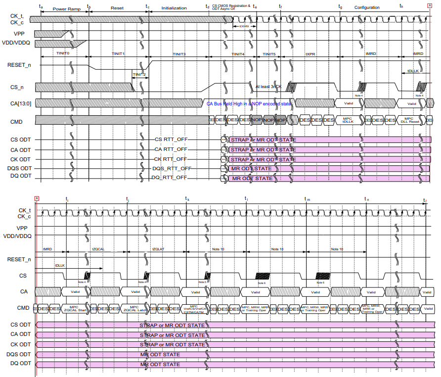
NOTES:
1) From time point (Td) until (Te), the command/address (CA) bus shall be held high in a NOP encoded state.
2) From time point (Te) until (Tf), NOP commands shall be applied on the command/address (CA) bus.
3) From time point (Tf) until (Tk), DES commands must be applied between legal commands (MRR, MRW, MPC, VREFCS & VREFCA). MRR and MRW command, while legal, may not execute properly until CS and CA training routines are completed.
4) Prior to ZQcal completion at (Tk), MPC commands shall be Multi-Cycle as described in the MPC command Timings section.
5) From time point (Tk) until (Tl) all MPC, VREFCS and VREFCA commands prior to CS and CA training successfully completing, shall be Multi-Cycle (MR2:OP[4]=0) as described in the MPC, VREFCS, and VREFCA timing sections.
6) At time point (Tl), with successful completion of CS and CA training, an MRW command setting MR2:OP[4] =1 is recommended and allows for MPC, VREFCS, VREFCA commands to be single-cycle, improving training duration.
7) From time point (Tk) until (Tz), DES commands shall be applied between legal commands (MRR, MRW, MPC, VREFCS & VREFCA).
8) Starting at TI, MRW Commands shall be issued to all Mode Registers that require defined settings.
9) Default ODT tolerances are wider prior to ZQ calibration.
10) All MPC/MRW/MRR to MPC/MRW/MRR commands shall meet the timing restrictions required.
NOTES:
1) Td부터 Te까지: 명령/주소 (CA) 버스는 NOP 인코딩 상태로 HIGH 상태로 유지되어야 합니다.
2) Te부터 Tf까지: CA 버스에 NOP 명령이 적용되어야 합니다.
3) Tf부터 Tk까지: 합법적인 명령 사이에 DES 명령이 적용되어야 하며, CS and CA training routines이 완료될 때까지 제대로 실행되지 않을 수 있습니다.
4) Tk 이전: MPC 명령은 Multi-Cycle로 처리되어야 합니다.
5) Tk부터 Tl까지: 특정 명령은 Multi-Cycle로 처리되어야 합니다.
6) Tl 시점: CS and CA training이 성공적으로 완료되면, 특정 설정이 권장되며, 일부 명령의 처리가 개선됩니다.
7) Tk부터 Tz까지: 합법적인 명령 사이에 DES 명령이 적용되어야 합니다.
8) TI부터 시작: 모든 모드 레지스터에 MRW 명령이 발행되어야 합니다.
9) ZQ calibration 전: 기본 ODT 허용 오차가 넓습니다.
10) 모든 MPC/MRW/MRR 명령: 필요한 타이밍 제한을 충족해야 합니다.
4. After RESET_n is de-asserted (Tc), wait at least tINIT3 before driving CS_n high.
4. RESET_n이 해제된 후 (Tc 시점), CS_n을 높은 상태로 전환하기 전에 최소한 tINIT3 시간 동안 기다려야 합니다.
5. After setting CS_n high (Td), wait a minimum of tINIT4 to allow the DRAM CMOS based receiver to register the exit and allow the CS_n, CK, CA, DQ and DQS ODT to go to the defined strap or MRS state (Te). Clock (CK_t, CK_c) is required to be started and stabilized for tCKSRX before exit of tINIT4 (Te). Upon the completion of Te, all ODT states (CA, CS_n, CK, DQ and DQS ODT) should be valid and the DRAM’s CS_n receiver should no longer be in its CMOS based mode. ODT termination states will be uncalibrated until completion of ZQcal at (Tj).
CS_n을 high 상태로 설정한 후 (Td 시점), DRAM의 CMOS 기반 receiver가 종료를 인식하고 CS_n, CK, CA, DQ 및 DQS ODT가 정의된 strap 또는 MRS 상태로 전환되도록 최소 tINIT4 시간 동안 기다려야 합니다 (Te 시점).
클럭 (CK_t, CK_c)은 tINIT4 (Te)의 종료 전에 시작되고 안정화되어야 합니다.
Te의 완료 시점에는 모든 ODT 상태 (CA, CS_n, CK, DQ 및 DQS ODT)가 유효해야 하며, DRAM의 CS_n receiver는 더 이상 CMOS 기반 모드에 있어서는 안 됩니다. ODT 종료 상태는 ZQcal이 완료될 때까지 (Tj 시점) 보정되지 않습니다.