
DDR2 SDRAM must be powered up and initialized in a predefined manner.
DDR2 SDRAM은 미리 정의된 방식으로 전원을 공급하고 초기화해야 합니다.
Operational procedures other than those specified may result in undefined operation.
지정된 절차 외의 작업 절차는 정의되지 않은 작업을 초래할 수 있습니다.
Figure 43 illustrates, and the notes outline, the sequence required for power-up and initialization.
Figure 43은 power-up 및 initialization에 필요한 순서를 보여주고, 주석은 그 순서를 개요로 설명합니다.
Power-Up and Initialization
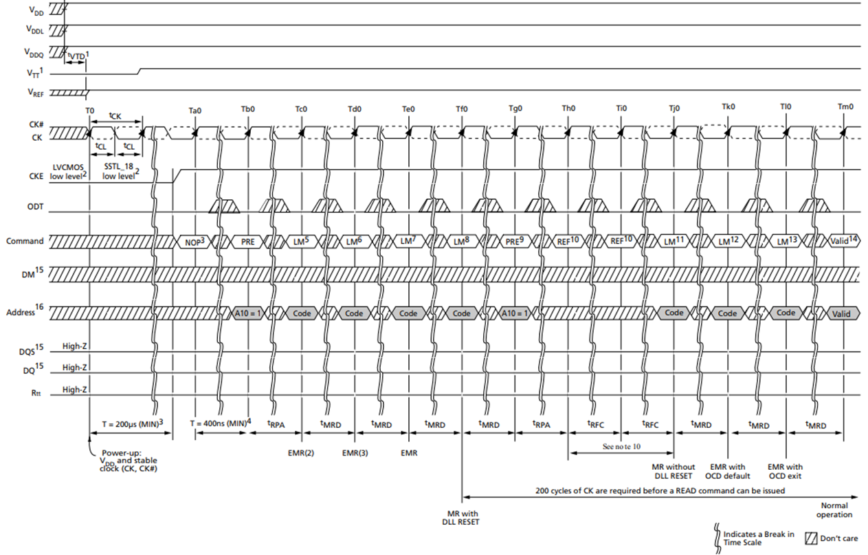
Applying power; if CKE is maintained below 0.2 × VDDQ, outputs remain disabled.
전원을 적용합니다. 만약 CKE가 0.2 × VDDQ 이하로 유지되면, 출력은 비활성화 상태를 유지합니다.
To guarantee RTT (ODT resistance) is off, VREF must be valid and a low level must be applied to the ODT ball (all other inputs may be undefined; I/Os and outputs must be less than VDDQ during voltage ramp time to avoid DDR2 SDRAM device latch-up).
RTT (ODT 저항)이 꺼져 있음을 보장하기 위해, VREF는 유효해야 하고 ODT 볼에는 낮은 레벨이 적용되어야 합니다 (다른 모든 입력은 정의되지 않을 수 있음; voltage ramp time 동안 I/O와 출력은 DDR2 SDRAM 장치의 latch-up을 피하기 위해 VDDQ보다 낮아야 합니다)."
→ VREF : 기준(reference)를 정해주는 전압(level)이 인가되는 핀
→ Voltage ramp time : 전원이 켜지거나 재설정 후에 장치가 안정적인 작동 상태에 도달하기까지 필요한 시간
→ latch-up : 과도한 전류가 흐르는 상태
→ VDDQ : I/O (입출력) 버스를 구동하는 데 사용되는 전압
VTT is not applied directly to the device; however, tVTD should be ≥ 0 to avoid device latch-up.
VTT는 장치에 직접 적용되지 않지만, 장치의 래치업을 피하기 위해 tVTD는 0 이상이어야 합니다.
→ VTT : Termination Voltage로 I/O (입출력) 버스에 연결된 저항의 양 끝에 적용되는 전압
→ tVTD : VTT가 장치에 적용되는 시간
→ tVTD가 너무 짧으면, 장치에 과도한 전압이 급격하게 적용될 수 있어 latch-up
At least one of the following two sets of conditions (A or B) must be met to obtain a stable supply state (stable supply defined as VDD, VDDL, VDDQ, VREF, and VTT are between their minimum and maximum values as stated in Table 13 (page 45)):
안정적인 공급 상태를 얻기 위해서는 다음 두 가지 조건 중 하나(A 또는 B)를 충족해야 합니다(안정적인 공급 상태란 VDD, VDDL, VDDQ, VREF, VTT가 table 13에 명시된 최소값과 최대값 사이에 있는 상태를 말합니다):
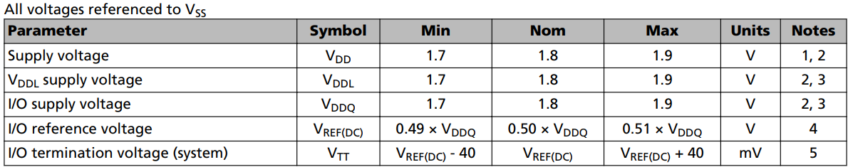
1. VDD and VDDQ must track each other. VDDQ must be ≤ VDD.
VDD와 VDDQ는 서로를 관찰해야 합니다. VDDQ는 VDD보다 작거나 같아야 합니다.
2. VSSQ = VSSL = VSS (MOSFET source)
3. VDDQ tracks with VDD; VDDL tracks with VDD.
3. VDDQ는 VDD를 따르고, VDDL 역시 VDD를 따라갑니다.
4. VREF is expected to equal VDDQ/2 of the transmitting device and to track variations in the DC level of the same. Peak-to-peak noise (noncommon mode) on VREF may not exceed ±1 percent of the DC value. Peak-to-peak AC noise on VREF may not exceed ±2 percent of VREF(DC). This measurement is to be taken at the nearest VREF bypass capacitor
VREF는 전송 장치의 VDDQ/2와 같아야 하며, 동일한 DC 수준의 변동을 추적해야 합니다. VREF의 피크-피크 노이즈(공통 모드가 아님)는 DC 값의 ±1%를 초과해서는 안 됩니다.VREF의 피크-피크 AC 노이즈는 VREF(DC)의 ±2%를 초과해서는 안 됩니다. 이 측정은 가장 가까운 VREF 바이패스 커패시터에서 이루어져야 합니다.
5. VTT is not applied directly to the device. VTT is a system supply for signal termination resistors, is expected to be set equal to VREF, and must track variations in the DC level of VREF.
5. VTT는 장치에 직접 적용되지 않습니다. VTT는 termination resistors을 위한 시스템 공급으로, VREF와 동일하게 설정되어야 하며, VREF의 DC 수준 변동을 추적해야 합니다.
A. Single power source: The VDD voltage ramp from 300mV to VDD,min must take no longer than 200ms; during the VDD voltage ramp, |VDD - VDDQ| ≤ 0.3V.
Once supply voltage ramping is complete (when VDDQ crosses VDD,min), Table 13 specifications apply.
A. Single power source: VDD 전압이 300mV에서 VDD,min까지 오르는 데 걸리는 시간은 200ms를 초과해서는 안됩니다. VDD 전압이 상승하는 동안 |VDD - VDDQ| ≤ 0.3V를 유지해야 합니다.
voltage ramping이 완료되면 (VDDQ가 VDD,min를 넘어갈 때), Table 13의 사양이 적용됩니다.
- VDD, VDDL, and VDDQ are driven from a single power converter output]
- VTT is limited to 0.95V MAX
- VREF tracks VDDQ/2; VREF must be within ±0.3V with respect to VDDQ/2 during supply ramp time; does not need to be satisfied when ramping power down
- VTT is limited to 0.95V MAX
목차 2에 해당하는 링크
목차 3에 해당하는 링크
목차 4에 해당하는 링크
DDR2 SDRAM must be powered up and initialized in a predefined manner.
DDR2 SDRAM은 미리 정의된 방식으로 전원을 공급하고 초기화해야 합니다.
Operational procedures other than those specified may result in undefined operation.
지정된 절차 외의 작업 절차는 정의되지 않은 작업을 초래할 수 있습니다.
Figure 43 illustrates, and the notes outline, the sequence required for power-up and initialization.
Figure 43은 power-up 및 initialization에 필요한 순서를 보여주고, 주석은 그 순서를 개요로 설명합니다.
Power-Up and Initialization
Applying power; if CKE is maintained below 0.2 × VDDQ, outputs remain disabled.
전원을 적용합니다. 만약 CKE가 0.2 × VDDQ 이하로 유지되면, 출력은 비활성화 상태를 유지합니다.
To guarantee RTT (ODT resistance) is off, VREF must be valid and a low level must be applied to the ODT ball (all other inputs may be undefined; I/Os and outputs must be less than VDDQ during voltage ramp time to avoid DDR2 SDRAM device latch-up).
RTT (ODT 저항)이 꺼져 있음을 보장하기 위해, VREF는 유효해야 하고 ODT 볼에는 낮은 레벨이 적용되어야 합니다 (다른 모든 입력은 정의되지 않을 수 있음; voltage ramp time 동안 I/O와 출력은 DDR2 SDRAM 장치의 latch-up을 피하기 위해 VDDQ보다 낮아야 합니다)."
→ VREF : 기준(reference)를 정해주는 전압(level)이 인가되는 핀
→ Voltage ramp time : 전원이 켜지거나 재설정 후에 장치가 안정적인 작동 상태에 도달하기까지 필요한 시간
→ latch-up : 과도한 전류가 흐르는 상태
→ VDDQ : I/O (입출력) 버스를 구동하는 데 사용되는 전압
VTT is not applied directly to the device; however, tVTD should be ≥ 0 to avoid device latch-up.
VTT는 장치에 직접 적용되지 않지만, 장치의 래치업을 피하기 위해 tVTD는 0 이상이어야 합니다.
→ VTT : Termination Voltage로 I/O (입출력) 버스에 연결된 저항의 양 끝에 적용되는 전압
→ tVTD : VTT가 장치에 적용되는 시간
→ tVTD가 너무 짧으면, 장치에 과도한 전압이 급격하게 적용될 수 있어 latch-up
At least one of the following two sets of conditions (A or B) must be met to obtain a stable supply state (stable supply defined as VDD, VDDL, VDDQ, VREF, and VTT are between their minimum and maximum values as stated in Table 13 (page 45)):
안정적인 공급 상태를 얻기 위해서는 다음 두 가지 조건 중 하나(A 또는 B)를 충족해야 합니다(안정적인 공급 상태란 VDD, VDDL, VDDQ, VREF, VTT가 table 13에 명시된 최소값과 최대값 사이에 있는 상태를 말합니다):
1. VDD and VDDQ must track each other. VDDQ must be ≤ VDD.
VDD와 VDDQ는 서로를 관찰해야 합니다. VDDQ는 VDD보다 작거나 같아야 합니다.
2. VSSQ = VSSL = VSS (MOSFET source)
3. VDDQ tracks with VDD; VDDL tracks with VDD.
3. VDDQ는 VDD를 따르고, VDDL 역시 VDD를 따라갑니다.
4. VREF is expected to equal VDDQ/2 of the transmitting device and to track variations in the DC level of the same. Peak-to-peak noise (noncommon mode) on VREF may not exceed ±1 percent of the DC value. Peak-to-peak AC noise on VREF may not exceed ±2 percent of VREF(DC). This measurement is to be taken at the nearest VREF bypass capacitor
VREF는 전송 장치의 VDDQ/2와 같아야 하며, 동일한 DC 수준의 변동을 추적해야 합니다. VREF의 피크-피크 노이즈(공통 모드가 아님)는 DC 값의 ±1%를 초과해서는 안 됩니다.VREF의 피크-피크 AC 노이즈는 VREF(DC)의 ±2%를 초과해서는 안 됩니다. 이 측정은 가장 가까운 VREF 바이패스 커패시터에서 이루어져야 합니다.
5. VTT is not applied directly to the device. VTT is a system supply for signal termination resistors, is expected to be set equal to VREF, and must track variations in the DC level of VREF.
5. VTT는 장치에 직접 적용되지 않습니다. VTT는 termination resistors을 위한 시스템 공급으로, VREF와 동일하게 설정되어야 하며, VREF의 DC 수준 변동을 추적해야 합니다.
A. Single power source: The VDD voltage ramp from 300mV to VDD,min must take no longer than 200ms; during the VDD voltage ramp, |VDD - VDDQ| ≤ 0.3V.
Once supply voltage ramping is complete (when VDDQ crosses VDD,min), Table 13 specifications apply.
A. Single power source: VDD 전압이 300mV에서 VDD,min까지 오르는 데 걸리는 시간은 200ms를 초과해서는 안됩니다. VDD 전압이 상승하는 동안 |VDD - VDDQ| ≤ 0.3V를 유지해야 합니다.
voltage ramping이 완료되면 (VDDQ가 VDD,min를 넘어갈 때), Table 13의 사양이 적용됩니다.
- VDD, VDDL, and VDDQ are driven from a single power converter output]
- VTT is limited to 0.95V MAX
- VREF tracks VDDQ/2; VREF must be within ±0.3V with respect to VDDQ/2 during supply ramp time; does not need to be satisfied when ramping power down
- VTT is limited to 0.95V MAX
목차 2에 해당하는 링크
목차 3에 해당하는 링크
목차 4에 해당하는 링크