
반응형
반가산기 설계
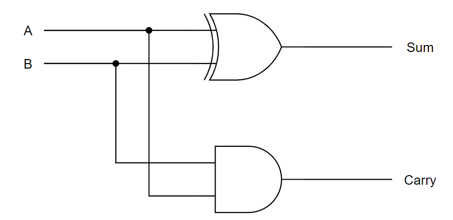
| 입력 | 출력 | ||
| A | B | sum | carry |
| 0 | 0 | 0 | 0 |
| 0 | 1 | 0 | 1 |
| 1 | 0 | 0 | 1 |
| 1 | 1 | 1 | 0 |
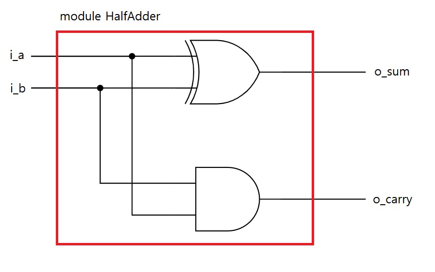
Design Source
`timescale 1ns / 1ps

module HalfAdder(
    input i_a,
    input i_b,

    output o_sum, o_carry
);

    assign o_sum  =   i_a ^ i_b;  // xor
    assign o_carry = i_a & i_b;   // and

endmoduleSimulation Source
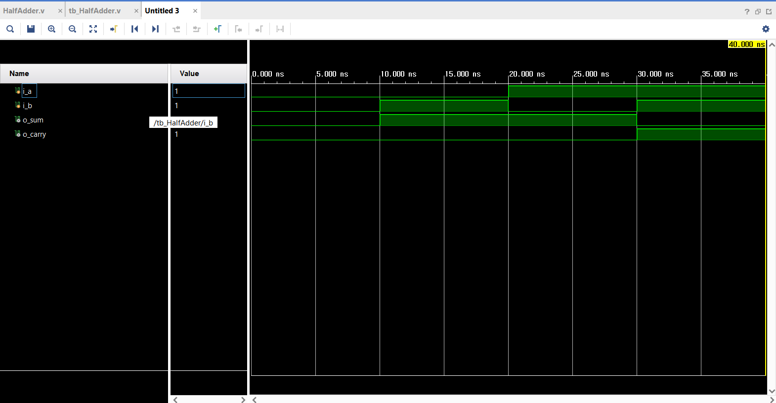
`timescale 1ns / 1ps
module tb_HalfAdder();
reg i_a, i_b;
wire o_sum, o_carry;
HalfAdder dut(
.i_a(i_a),
.i_b(i_b),
.o_sum(o_sum),
.o_carry(o_carry)
);
initial begin
#00 i_a = 1'b0; i_b = 1'b0;
#10 i_a = 1'b0; i_b = 1'b1;
#10 i_a = 1'b1; i_b = 1'b0;
#10 i_a = 1'b1; i_b = 1'b1;
#10 $finish;
end
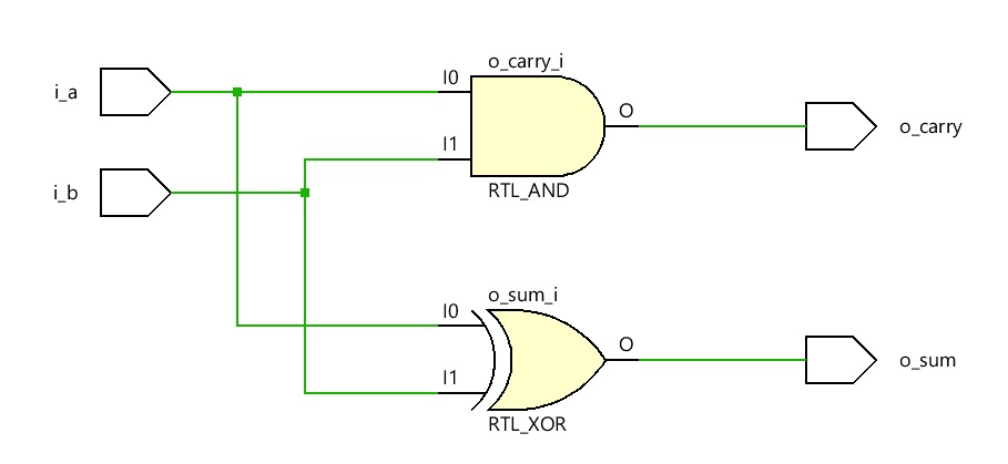
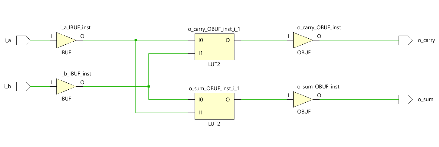
endmoduleSchematic
Timing Chart
constraints
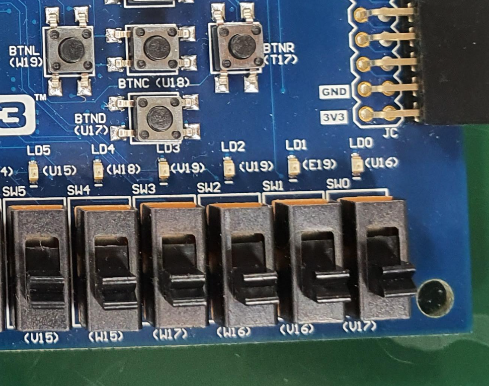
## Switches
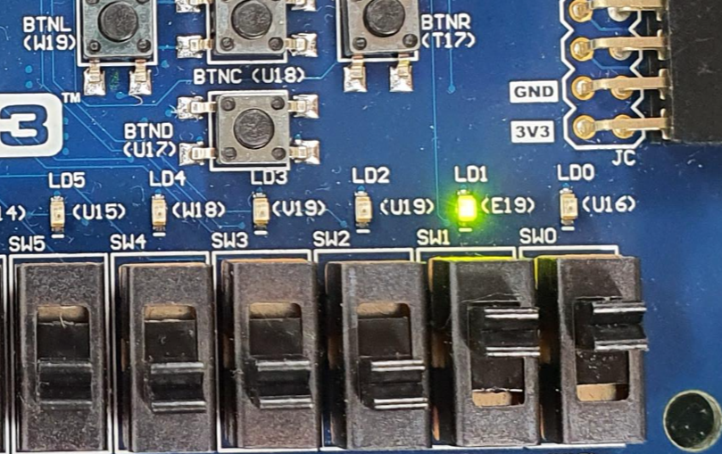
set_property -dict { PACKAGE_PIN V17 IOSTANDARD LVCMOS33 } [get_ports { i_a }]; #IO_L19N_T3_A09_D25_VREF_14 ,Sch=SW0
set_property -dict { PACKAGE_PIN V16 IOSTANDARD LVCMOS33 } [get_ports { i_b }]; #IO_L19P_T3_A10_D26_14 ,Sch=SW1
## LEDs
set_property -dict { PACKAGE_PIN U16 IOSTANDARD LVCMOS33 } [get_ports { o_sum}]; #IO_L23N_T3_A02_D18_14 ,Sch=LED0
set_property -dict { PACKAGE_PIN E19 IOSTANDARD LVCMOS33 } [get_ports { o_carry}]; #IO_L3N_T0_DQS_EMCCLK_14 ,Sch=LED1
## Configuration options, can be used for all designs
set_property CONFIG_VOLTAGE 3.3 [current_design]
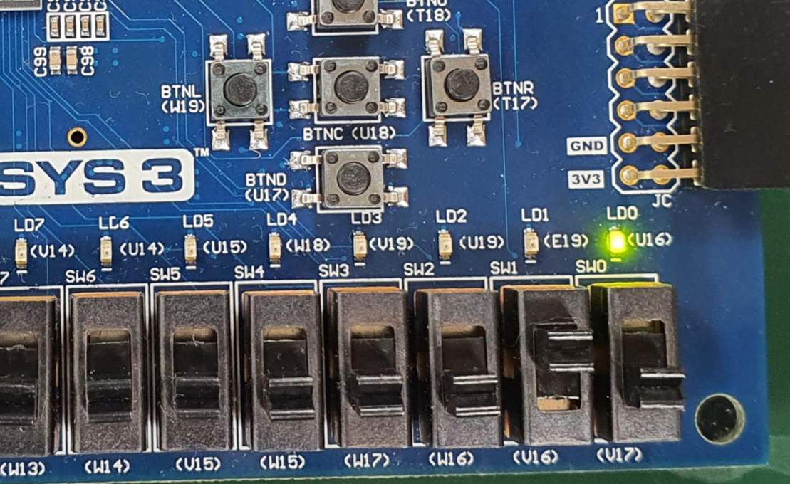
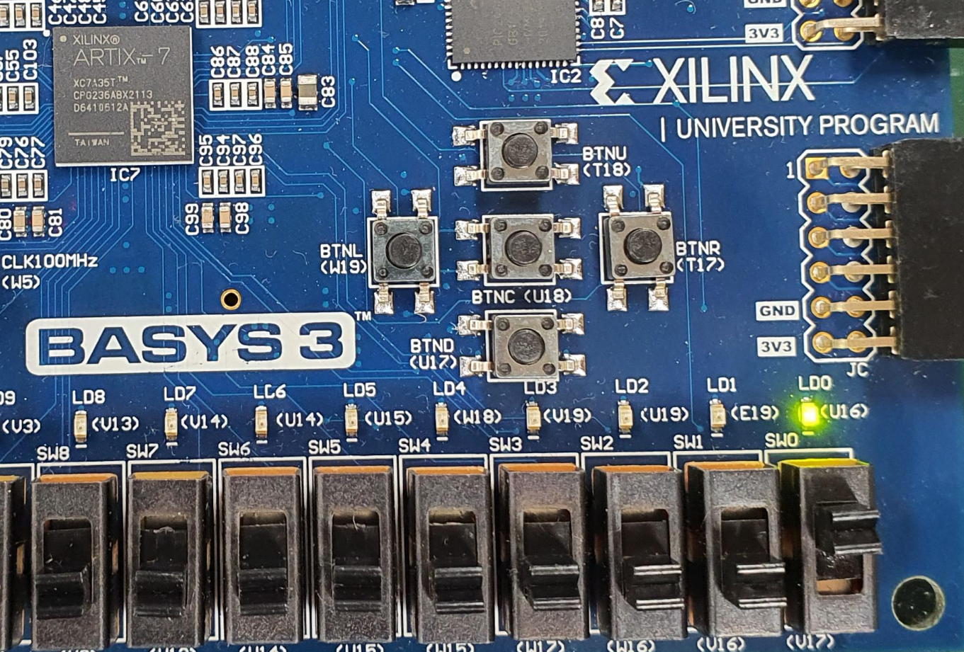
set_property CFGBVS VCCO [current_design]반가산기 FPGA 회로 구성
작동사진
반응형
반응형
반가산기 설계
| 입력 | 출력 | ||
| A | B | sum | carry |
| 0 | 0 | 0 | 0 |
| 0 | 1 | 0 | 1 |
| 1 | 0 | 0 | 1 |
| 1 | 1 | 1 | 0 |
Design Source
`timescale 1ns / 1ps

module HalfAdder(
    input i_a,
    input i_b,

    output o_sum, o_carry
);

    assign o_sum  =   i_a ^ i_b;  // xor
    assign o_carry = i_a & i_b;   // and

endmodule
Simulation Source
`timescale 1ns / 1ps

module tb_HalfAdder();

    reg i_a, i_b;
    wire o_sum, o_carry;

    HalfAdder dut(
    .i_a(i_a),
    .i_b(i_b),
    .o_sum(o_sum),
    .o_carry(o_carry)
    );

    initial begin
        #00 i_a = 1'b0; i_b = 1'b0;
        #10 i_a = 1'b0; i_b = 1'b1;
        #10 i_a = 1'b1; i_b = 1'b0;
        #10 i_a = 1'b1; i_b = 1'b1;
        #10 $finish;
    end

endmodule
Schematic
Timing Chart
constraints
## Switches

set_property -dict { PACKAGE_PIN V17  IOSTANDARD LVCMOS33 } [get_ports { i_a }]; #IO_L19N_T3_A09_D25_VREF_14 ,Sch=SW0
set_property -dict { PACKAGE_PIN V16  IOSTANDARD LVCMOS33 } [get_ports { i_b }]; #IO_L19P_T3_A10_D26_14      ,Sch=SW1

## LEDs

set_property -dict { PACKAGE_PIN U16  IOSTANDARD LVCMOS33 } [get_ports { o_sum}]; #IO_L23N_T3_A02_D18_14        ,Sch=LED0
set_property -dict { PACKAGE_PIN E19  IOSTANDARD LVCMOS33 } [get_ports { o_carry}]; #IO_L3N_T0_DQS_EMCCLK_14      ,Sch=LED1

## Configuration options, can be used for all designs
set_property CONFIG_VOLTAGE 3.3 [current_design]
set_property CFGBVS VCCO [current_design]
반가산기 FPGA 회로 구성
작동사진
반응형